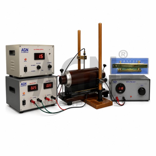
This experimental setup is designed to study the phenomenon of magnetoresistance, which refers to the change in electrical resistance of a material when it is subjected to an external magnetic field. When a magnetic field is applied to a semiconductor sample, the motion of charge carriers is influenced by the Lorentz force, causing their paths to deviate from a straight line. Since charge carriers within the material possess different drift velocities, the applied magnetic field affects them differently. Some carriers become overcompensated while others are undercompensated, resulting in altered trajectories and increased scattering. This effectively reduces the mean free path of the charge carriers, leading to an increase in the resistivity of the material. By measuring the variation in resistance with magnetic field strength, students can investigate the magnetoresistance effect and gain insight into charge transport mechanisms in semiconductors. The experiment provides a practical understanding of semiconductor physics, carrier dynamics, and the influence of magnetic fields on electrical conduction.
Features
Four-probe arrangement for accurate resistance measurement.
High-quality p-type Germanium (Ge) sample.
Complete magnetoresistance experimental setup.
Heavy-duty electromagnet capable of producing magnetic fields up to 7.5 kG.
Constant current power supply for stable and precise measurements.
Digital Gauss Meter with measurement range up to 20 kG.
Suitable for advanced studies in semiconductor physics and solid-state electronics.
Apparatus Included
Four-Probe Measurement Assembly
p-Type Germanium Sample
Magnetoresistance Experimental Unit
Electromagnet (7.5 kG)
Constant Current Power Supply
Digital Gauss Meter (20 kG Range)
Connecting Cables and Accessories
Educational Applications
Study of magnetoresistance in semiconductors.
Investigation of the effect of magnetic field on electrical resistance.
Analysis of charge carrier transport mechanisms.
Understanding Lorentz force and carrier scattering effects.
Practical demonstration of solid-state and semiconductor physics concepts.
This setup is widely used in physics laboratories, engineering colleges, and research institutions for experiments related to semiconductor characterization, electronic materials, and magnetic field effects on electrical conduction.