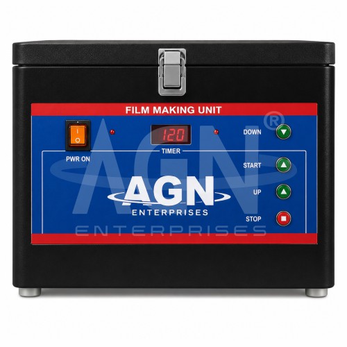
The Film Making Unit from AGN Enterprises is a practical PCB fabrication system designed for preparing circuit artwork films used during printed circuit board production. It provides students, technicians, and electronics developers with a convenient solution for creating and processing suitable PCB films before transferring the required circuit pattern onto a photosensitive board.
In PCB fabrication, accurate artwork plays an important role because it defines the conductive tracks, pads, and other circuit features that appear on the finished board. Therefore, proper film preparation helps users achieve clear circuit patterns during the subsequent exposure and development processes.
The unit supports practical work involving PCB artwork preparation, film processing, circuit pattern development, positive or negative artwork, and photographic PCB fabrication techniques, depending on the supplied configuration. Moreover, students can understand how a designed circuit layout progresses from artwork to film and finally to a physical printed circuit board.
After preparing the required film, users can position it with a photosensitive PCB and carry out UV exposure. Subsequently, they can develop and etch the board to obtain the required copper pattern. Consequently, the equipment helps students understand the relationship between artwork quality, exposure, development, and final PCB results.
For additional information about printed circuit board manufacturing practices and electronics industry standards, users can refer to IPC.
The Film Making Unit complements other PCB fabrication equipment such as artwork tables, photoresist coating machines, UV exposure machines, developer units, etching machines, curing ovens, drilling machines, and PCB shearing equipment. Furthermore, this integrated workflow gives students practical exposure to multiple PCB manufacturing stages.