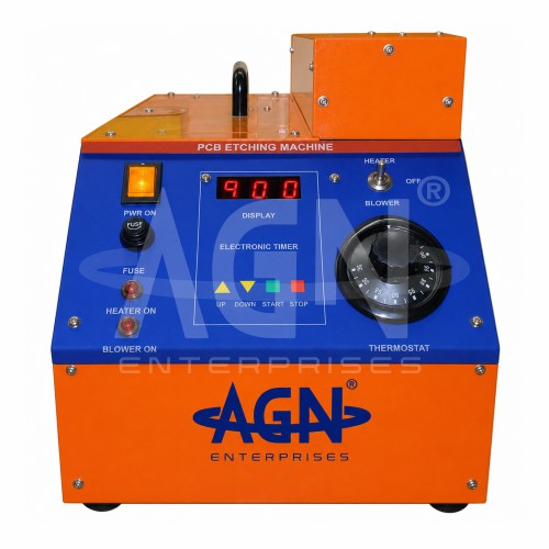
The PCB Etching Machine from AGN Enterprises is a practical electronics laboratory and PCB fabrication unit designed for the controlled etching of printed circuit boards during circuit development and prototyping. It helps students, technicians, and developers remove unwanted copper from prepared PCB material while retaining the required circuit pattern.
During PCB fabrication, users first transfer the required circuit artwork onto a copper-clad board using a suitable resist process. After development, they place the prepared board into an appropriate etching solution. Therefore, the exposed unwanted copper dissolves while the protected copper remains to form the required conductive tracks and pads.
Moreover, the machine provides a dedicated arrangement for performing the etching process more conveniently than basic manual methods. Depending on the supplied configuration, suitable solution circulation or agitation can support more uniform contact between the etchant and board surface. Consequently, users can achieve controlled processing while gaining practical knowledge of PCB artwork transfer, developing, etching, track formation, drilling, and final board preparation.
The equipment integrates effectively with other PCB laboratory machines such as an artwork table, UV exposure unit, dye and developer unit, PCB shearing equipment, and drilling machine. Furthermore, this complete workflow helps students understand each major stage of printed circuit board production.
For additional information about PCB manufacturing practices and electronics industry standards, users can refer to IPC.
The PCB Etching Machine provides a practical solution for educational institutes, R&D laboratories, electronics workshops, and prototype development facilities. In addition, its dedicated processing arrangement supports organized PCB fabrication activities.